Table of Content
This page provides detailed information on the LM741CN operational amplifier, covering the LM741CN pinout diagram, pin configuration, pin description, schematic, functional block diagram, typical circuit, and layout example for electronics engineers.
1. LM741CN Description
The LM741CN series are general-purpose operational amplifiers with improved performance over industry standards like the LM709. They serve as direct replacements for the 709C, LM201, MC1439, and 748 in most applications. The LM741CN operates over a 0°C to +70°C temperature range, unlike the -55°C to +125°C range of LM741 and LM741A.
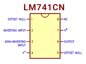
2. LM741CN Pinout Diagram
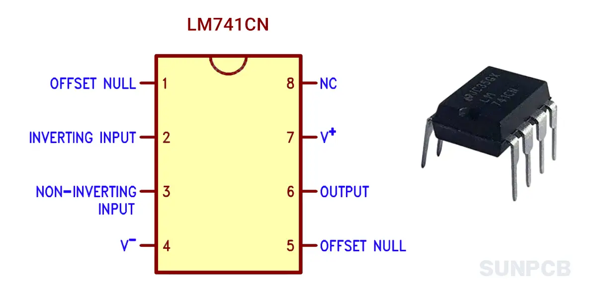
![]() LM741CN pinout diagram pdf download (P3/P18)
LM741CN pinout diagram pdf download (P3/P18)
3. LM741CN Pin Configuration and Description
| Pin Number | Pin Name | Type | Pinout Description |
|---|---|---|---|
| 1 | Offset Null | I | Offset null pin used to eliminate offset voltage and balance input voltages |
| 2 | Inverting Input | I | Inverting signal input |
| 3 | Noninverting Input | I | Noninverting signal input |
| 4 | V- | I | Negative supply voltage |
| 5 | Offset Null | I | Offset null pin used to eliminate offset voltage and balance input voltages |
| 6 | Output | O | Amplified signal output |
| 7 | V+ | I | Positive supply voltage |
| 8 | NC | N/A | No Connect, should be left floating |
4. LM741CN Features
- Overload protection on input and output
- No latch-up when common-mode range is exceeded
- Freedom from oscillations
5. LM741CN Applications
Comparators; Multivibrators; DC Amplifiers; Summing Amplifiers; Integrators or Differentiators; Active Filters
6. LM741CN Typical Application Circuit
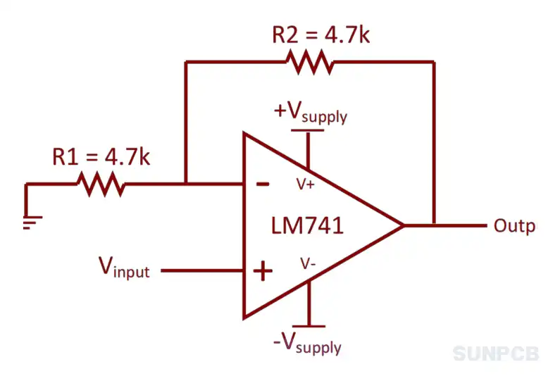
LM741CN Noninverting Amplifier Circuit, located on Page 9.
This circuit uses a noninverting configuration with a gain of 2, set by 4.7-kΩ resistors. Engineers should use 1% tolerance resistors for accurate gain and decouple power supplies with 0.1µF capacitors to reduce noise.
7. LM741CN Functional Block Diagram
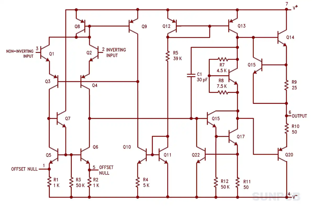
LM741CN Functional Block Diagram Located on Page 7. ![]() LM741CN functional block diagram pdf download (P7/P18)
LM741CN functional block diagram pdf download (P7/P18)
Key Points
- Input stage handles differential signals with high gain.
- Amplification stage boosts signal for output.
- Output stage delivers amplified signal with low impedance.
8. LM741CN Layout Example
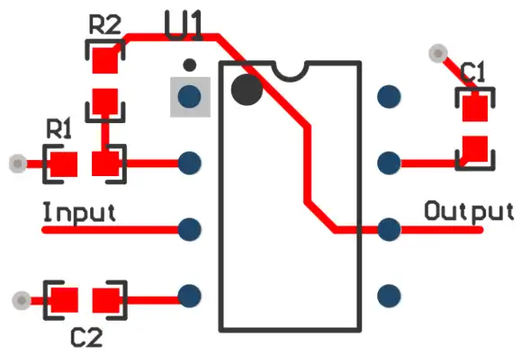
LM741CN Layout Example Located on Page 11.  LM741CN Layout (P11/P18)
Key Points
- Place feedback resistors close to inputs to minimize noise.
- Position decoupling capacitors near power pins for stability.
- Optimize component placement to reduce parasitic capacitance.
9. LM741CN Package Example Dimension - TO-99-8, CDIP-8, PDIP-8
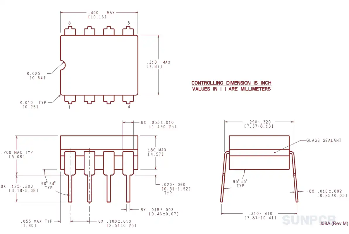
LM741CN Package Example Dimension Located on Pages 15-17.
![]() LM741CN Layout (P15-17/P18)
LM741CN Layout (P15-17/P18)
These pages detail mechanical dimensions for TO-99, CDIP, and PDIP packages. Engineers must verify package compatibility with their PCB design and ensure proper soldering conditions (260°C for PDIP, 300°C for CDIP/TO-99).
10. LM741CN Electrical Characteristics
| Parameter | Test Conditions | Min | Typ | Max | Unit |
|---|---|---|---|---|---|
| Input offset voltage | RS ≤ 10 kΩ, TA = 25°C | 2 | 6 | mV | |
| Input offset voltage | RS ≤ 10 kΩ, TAMIN ≤ TA ≤ TAMAX | 7.5 | mV | ||
| Input offset voltage adjustment range | TA = 25°C, VS = ±20 V | ±15 | mV | ||
| Input offset current | TA = 25°C | 20 | 200 | nA | |
| Input offset current | TAMIN ≤ TA ≤ TAMAX | 300 | nA | ||
| Input bias current | TA = 25°C | 80 | 500 | nA | |
| Input bias current | TAMIN ≤ TA ≤ TAMAX | 0.8 | µA | ||
| Input resistance | TA = 25°C, VS = ±20 V | 0.3 | 2 | MΩ | |
| Input voltage range | TA = 25°C | ±12 | ±13 | V | |
| Large signal voltage gain | VS = ±15 V, VO = ±10 V, RL ≥ 2 kΩ, TA = 25°C | 20 | 300 | V/mV | |
| Large signal voltage gain | VS = ±15 V, VO = ±10 V, RL ≥ 2 kΩ, TAMIN ≤ TA ≤ TAMAX | 15 | V/mV | ||
| Output voltage swing | VS = ±15 V, RL ≥ 10 kΩ | ±12 | ±14 | V | |
| Output voltage swing | VS = ±15 V, RL ≥ 2 kΩ | ±10 | ±13 | V | |
| Output short circuit current | TA = 25°C | 25 | mA | ||
| Common-mode rejection ratio | RS ≤ 10 kΩ, VCM = ±12 V, TAMIN ≤ TA ≤ TAMAX | 70 | 90 | dB | |
| Supply voltage rejection ratio | VS = ±20 V to VS = ±5 V, RS ≤ 10 kΩ, TAMIN ≤ TA ≤ TAMAX | 77 | 96 | dB | |
| Transient response (Rise time) | TA = 25°C, Unity Gain | 0.3 | µs | ||
| Transient response (Overshoot) | TA = 25°C, Unity Gain | 5% | |||
| Slew rate | TA = 25°C, Unity Gain | 0.5 | V/µs | ||
| Supply current | TA = 25°C | 1.7 | 2.8 | mA | |
| Power consumption | VS = ±15 V, TA = 25°C | 50 | 85 | mW |
These parameters are critical for LM741 schematic design. Ensure operating conditions align with specifications.
11. LM741CN Design Considerations
- Do not exceed ±22V supply voltage for LM741/LM741A or ±18V for LM741C.
- Use 0.1µF capacitors near power pins for decoupling.
- Derate power dissipation at high temperatures based on thermal resistance.
12. LM741CN FAQs and Tips
FAQs
Q: What is the supply voltage range for LM741?
A: LM741 and LM741A support ±10V to ±22V; LM741C supports ±10V to ±18V.
Q: Can LM741CN be used as a comparator?
A: Yes, in open-loop mode, it compares input voltages and outputs high or low.
Q: How to reduce noise in LM741CN circuits?
A: Use 0.1µF decoupling capacitors near power pins and keep feedback resistors close to the chip.
Q: What is the purpose of offset null pins?
A: They adjust input offset voltage for balanced inputs.
Q: Is LM741CN suitable for high-frequency applications?
A: No, its 1.5 MHz bandwidth limits high-frequency performance.
Tips
- Use 1% resistors for precise gain control.
- Connect offset null pins with a potentiometer to minimize offset voltage.
- Place decoupling capacitors to reduce power supply noise.
- Avoid high-frequency signals due to limited bandwidth.