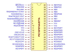
PIC16F877A-I/P Pinout Diagram and Overview
The PIC16F877A-I/P is a specific variant of the PIC16F877A microcontroller from Microchip Technology. The PIC16F877A refers to the general model, an 8-bit, 40-pin microcontroller with 8K Flash, 368 bytes RAM, and versatile peripherals. The -I/P suffix indicates the industrial temperature range (-40°C to +85°C) and PDIP (40-pin Plastic Dual Inline Package) packaging. Functionally, PIC16F877A-I/P is identical to other PIC16F877A variants (e.g., -I/PT, -I/L, -I/ML), differing only in its through-hole PDIP package, ideal for prototyping and manual assembly. Refer to the PIC16F877A datasheet (Section 17.0) for package details.
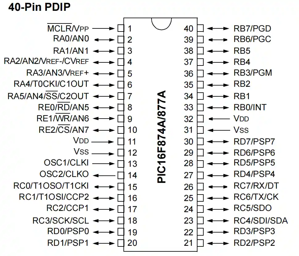
PIC16F877A-I/P Pinout Diagram(PDIP-40) Download pdf - P3/P234
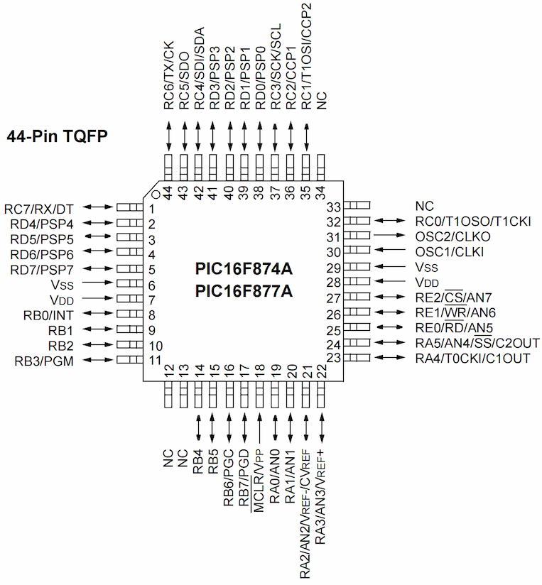
PIC16F877A-I/PT Pinout Diagram(TQFP-44) Download pdf - P3/P234
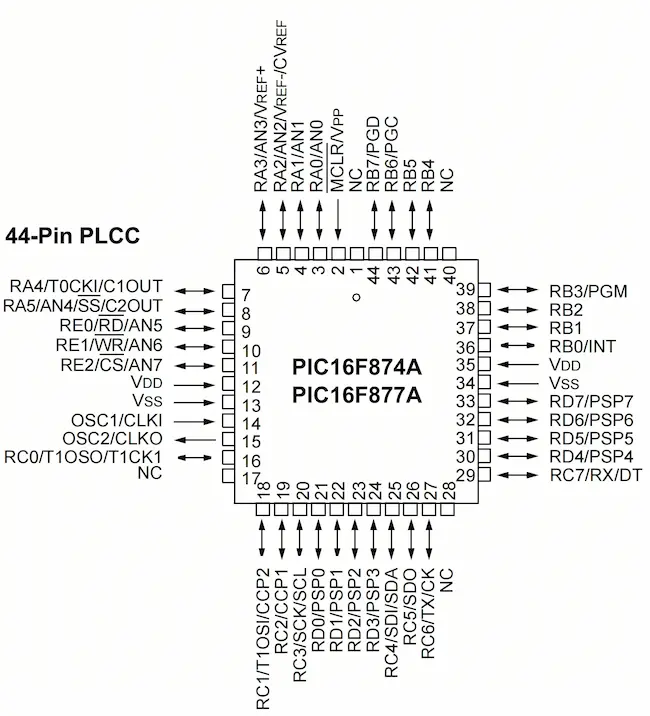
PIC16F877A-I/L Pinout Diagram(PLCC-44) Download pdf - P3/P234
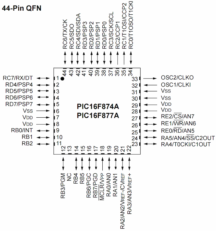
PIC16F877A-I/ML Pinout Diagram(QFN-44) Download pdf - P3/P234
| Criteria | PIC16F877A-I/P PDIP-40 |
PIC16F877A-I/PT TQFP-44 |
PIC16F877A-I/L PLCC-44 |
PIC16F877A-I/ML QFN-44 |
|---|---|---|---|---|
| Pin Count (Model) | 40 | 44 (4 NC pins) | 44 (4 NC pins) | 44 (4 NC pins) |
| Dimensions (mm, Model) | 52.26 x 13.84 x 4.06 | 10 x 10 x 1.0 | 16.59 x 16.59 x 4.57 | 8 x 8 x 0.9 |
| Pitch (mm, Model) | 2.54 (100 mil) | 0.8 | 1.27 (50 mil) | 0.5 |
| Mounting Type (Model) | Through-Hole | Surface-Mount | Surface-Mount (Socketable) | Surface-Mount |
| Key Features & Applications (Model) | Wide pin spacing, easy prototyping, robust for hobbyist/industrial use | Compact, low-profile, ideal for space-constrained designs | Square footprint, socketable, suited for legacy systems | Ultra-compact, excellent thermal performance, high-density PCBs |
| Typical Use Case (Model) | Prototyping, educational projects, low-cost industrial control | Consumer electronics, compact IoT devices | Automotive modules, legacy industrial systems | Portable devices, advanced IoT applications |
| Functional Differences (Model) | All 40 pins fully functional; no NC pins; ICSP on RB6/RB7, LVP on RB3 configurable | 4 NC pins (no function); same pinout for active pins; ICSP/LVP identical | 4 NC pins; socketable for easy reprogramming; ICSP/LVP unchanged | 4 NC pins; exposed pad for grounding; ICSP/LVP same but requires precise PCB layout |
| Performance Differences (Model) | Higher thermal resistance (~70°C/W); suited for low-power, 20 MHz operation | Moderate thermal resistance (~50°C/W); reliable at 20 MHz in compact designs | Moderate thermal resistance (~45°C/W); stable for 20 MHz, legacy high-current use | Low thermal resistance (~30°C/W); best for high-frequency 20 MHz, high-power applications |
PIC16F877A-I/P & PIC16F877A-I/PT PINOUT DESCRIPTION
| Pin Name | -I/P PDIP-40 Pin# |
I/PT PLCC-44 Pin# |
-I/L TQFP-44 Pin# |
-I/ML QFN-44 Pin# |
I/O/P Type |
Buffer Type |
Description |
|---|---|---|---|---|---|---|---|
| OSC1/CLKI OSC1 CLKI |
13 | 14 | 30 | 32 | I I |
ST/CMOS(3) | Oscillator crystal or external clock input. |
| OSC2/CLKO OSC2 CLKO |
14 | 15 | 31 | 33 | O O |
— | Oscillator crystal or clock output. |
| MCLR/VPP MCLR VPP |
1 | 2 | 18 | 18 | I P |
ST | Master Clear (input) or programming voltage (output). |
| PIC16F877A PORTA is a bidirectional I/O port. | |||||||
| Pin Name | PDIP-40 Pin# |
PLCC-44 Pin# |
TQFP-44 Pin# |
QFN-44 Pin# |
I/O/P Type |
Buffer Type |
Description |
| RA0/AN0 RA0 AN0 |
2 | 3 | 19 | 19 | I/O I |
TTL | Digital I/O. Analog input 0. |
| RA1/AN1 RA1 AN1 |
3 | 4 | 20 | 20 | I/O I |
TTL | Digital I/O. Analog input 1. |
| RA2/AN2/VREF-/CVREF RA2 AN2 VREF- CVREF |
4 | 5 | 21 | 21 | I/O I I O |
TTL | Digital I/O. Analog input 2. A/D reference voltage (Low) input. Comparator VREF output. |
| RA3/AN3/VREF+ RA3 AN3 VREF+ |
5 | 6 | 22 | 22 | I/O I I |
TTL | Digital I/O. Analog input 3. A/D reference voltage (High) input. |
| RA4/T0CKI/C1OUT RA4 T0CKI C1OUT |
6 | 7 | 23 | 23 | I/O I O |
ST | Digital I/O - Open-drain when configured as output. Timer0 external clock input. Comparator 1 output. |
| RA5/AN4/SS/C2OUT RA5 AN4 SS C2OUT |
7 | 8 | 24 | 24 | I/O I I O |
TTL | Digital I/O. Analog input 4. SPI slave select input. Comparator 2 output. |
| PIC16F877A PORTB is a bidirectional I/O port. PORTB can be software programmed for internal weak pull-up on all inputs. | |||||||
| Pin Name | PDIP-40 Pin# |
PLCC-44 Pin# |
TQFP-44 Pin# |
QFN-44 Pin# |
I/O/P Type |
Buffer Type |
Description |
| RB0/INT RB0 INT |
33 | 36 | 8 | 9 | I/O I |
TTL/ST(1) | Digital I/O. External interrupt. |
| RB1 | 34 | 37 | 9 | 10 | I/O | TTL | Digital I/O. |
| RB2 | 35 | 38 | 10 | 11 | I/O | TTL | Digital I/O. |
| RB3/PGM RB3 PGM |
36 | 39 | 11 | 12 | I/O I |
TTL | Digital I/O. Low-voltage ICSP programming enable pin. |
| RB4 | 37 | 41 | 14 | 14 | I/O | TTL | Digital I/O. |
| RB5 | 38 | 42 | 15 | 15 | I/O | TTL | Digital I/O. |
| RB6/PGC RB6 PGC |
39 | 43 | 16 | 16 | I/O I |
TTL/ST(2) | Digital I/O. In-circuit debugger and ICSP programming clock. |
| RB7/PGD RB7 PGD |
40 | 44 | 17 | 17 | I/O I/O |
TTL/ST(2) | Digital I/O. In-circuit debugger and ICSP programming data. |
| PIC16F877A PORTC is a bidirectional I/O port. | |||||||
| Pin Name | PDIP-40 Pin# |
PLCC-44 Pin# |
TQFP-44 Pin# |
QFN-44 Pin# |
I/O/P Type |
Buffer Type |
Description |
| RC0/T1OSO/T1CKI RC0 T1OSO T1CKI |
15 | 16 | 32 | 34 | I/O O I |
ST | Digital I/O. Timer1 oscillator output. Timer1 external clock input. |
| RC1/T1OSI/CCP2 RC1 T1OSI CCP2 |
16 | 18 | 35 | 35 | I/O I I/O |
ST | Digital I/O. Timer1 oscillator input. Capture2 input, Compare2 output, PWM2 output. |
| RC2/CCP1 RC2 CCP1 |
17 | 19 | 36 | 36 | I/O I/O |
ST | Digital I/O. Capture1 input, Compare1 output, PWM1 output. |
| RC3/SCK/SCL RC3 SCK SCL |
18 | 20 | 37 | 37 | I/O I/O I/O |
ST | Digital I/O. Synchronous serial clock input/output for SPI mode. Synchronous serial clock input/output for I2C mode. |
| RC4/SDI/SDA RC4 SDI SDA |
23 | 25 | 42 | 42 | I/O I I/O |
ST | Digital I/O. SPI data in. I2C data I/O. |
| RC5/SDO RC5 SDO |
24 | 26 | 43 | 43 | I/O O |
ST | Digital I/O. SPI data out. |
| RC6/TX/CK RC6 TX CK |
25 | 27 | 44 | 44 | I/O O I/O |
ST | Digital I/O. USART asynchronous transmit. USART synchronous clock. |
| RC7/RX/DT RC7 RX DT |
26 | 29 | 1 | 1 | I/O I I/O |
ST | Digital I/O. USART asynchronous receive. USART synchronous data. |
| PIC16F877A PORTD is a bidirectional I/O port or Parallel Slave Port when interfacing to a microprocessor bus. | |||||||
| Pin Name | PDIP-40 Pin# |
PLCC-44 Pin# |
TQFP-44 Pin# |
QFN-44 Pin# |
I/O/P Type |
Buffer Type |
Description |
| RD0/PSP0 RD0 PSP0 |
19 | 21 | 38 | 38 | I/O I/O | ST/TTL(3) | Digital I/O. Parallel Slave Port data. |
| RD1/PSP1 RD1 PSP1 |
20 | 22 | 39 | 39 | I/O I/O | ST/TTL(3) | Digital I/O. Parallel Slave Port data. |
| RD2/PSP2 RD2 PSP2 |
21 | 23 | 40 | 40 | I/O I/O | ST/TTL(3) | Digital I/O. Parallel Slave Port data. |
| RD3/PSP3 RD3 PSP3 |
22 | 24 | 41 | 41 | I/O I/O | ST/TTL(3) | Digital I/O. Parallel Slave Port data. |
| RD4/PSP4 RD4 PSP4 |
27 | 30 | 2 | 2 | I/O I/O | ST/TTL(3) | Digital I/O. Parallel Slave Port data. |
| RD5/PSP5 RD5 PSP5 |
28 | 31 | 3 | 3 | I/O I/O | ST/TTL(3) | Digital I/O. Parallel Slave Port data. |
| RD6/PSP6 RD6 PSP6 |
29 | 32 | 4 | 4 | I/O I/O | ST/TTL(3) | Digital I/O. Parallel Slave Port data. |
| RD7/PSP7 RD7 PSP7 |
30 | 33 | 5 | 5 | I/O I/O | ST/TTL(3) | Digital I/O. Parallel Slave Port data. |
| PIC16F877A PORTE is a bidirectional I/O port. | |||||||
| Pin Name | PDIP-40 Pin# |
PLCC-44 Pin# |
TQFP-44 Pin# |
QFN-44 Pin# |
I/O/P Type |
Buffer Type |
Description |
| RE0/RD/AN5 RE0 RD AN5 |
8 | 9 | 25 | 25 | I/O I I | ST/TTL(3) | Digital I/O. Read control for Parallel Slave Port. Analog input 5. |
| RE1/WR/AN6 RE1 WR AN6 |
9 | 10 | 26 | 26 | I/O I I | ST/TTL(3) | Digital I/O. Write control for Parallel Slave Port. Analog input 6. |
| RE2/CS/AN7 RE2 CS AN7 |
10 | 11 | 27 | 27 | I/O I I | ST/TTL(3) | Digital I/O. Chip select control for Parallel Slave Port. Analog input 7. |
| VSS | 12, 31 | 13, 34 | 6, 29 | 6, 30, 31 | P | — | Ground reference for logic and I/O pins. |
| VDD | 11, 32 | 12, 35 | 7, 28 | 7, 8, 28, 29 | P | — | Positive supply for logic and I/O pins. |
| NC | — | 1, 17, 28, 40 | 12, 13, 33, 34 | 13 | — | — | These pins are not internally connected |
Legend: I = input; O = output; I/O = input/output; P = power; — = Not used; TTL = TTL input; ST = Schmitt Trigger input
Note 1: This buffer is a Schmitt Trigger input when configured as the external interrupt.
Note 2: This buffer is a Schmitt Trigger input when used in Serial Programming mode.
Note 3: This buffer is a Schmitt Trigger input when configured in RC Oscillator mode and a CMOS input otherwise.