Table of Content
This page covers the STM32F051R8T6 microcontroller. Find the STM32F051R8T6 Pinout Diagram, STM32F051R8T6 pin configuration, STM32F051R8T6 pin description, schematic, and diagram details below. Key info for circuit design is included.
1. STM32F051R8T6 Pinout Diagram
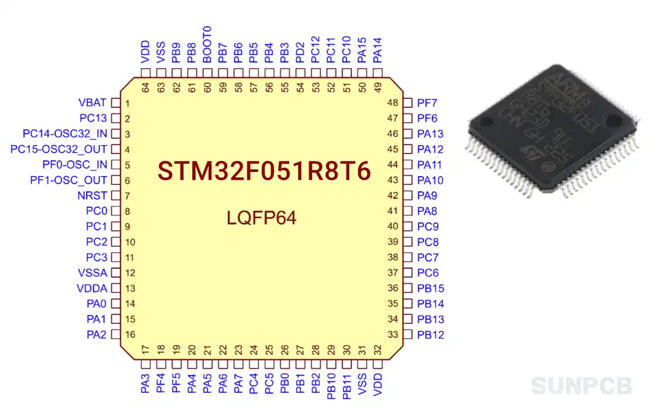
STM32F051R8T6 Pinout Diagram. Shows pin layout. Located on page 27.
![]() STM32F051R8T6 pinout diagram pdf download (P27/P122)
STM32F051R8T6 pinout diagram pdf download (P27/P122)
2. STM32F051R8T6 Pin Configuration and Description
| Pin # | Pin Name | Type | I/O Structure | Alternate Functions | Additional Functions | Pin Description |
|---|---|---|---|---|---|---|
| 1 | VBAT | S | - | - | - | Backup power supply for RTC, external clock, and backup registers when VDD is not present. |
| 2 | PC13 | I/O | TC | - | RTC_TAMP1, RTC_TS, RTC_OUT, WKUP2 | Port C, Pin 13. Can be used for RTC tamper detection, timestamp, RTC output, or Wakeup event. Supplied through power switch, limited output capability. |
| 3 | PC14-OSC32_IN | I/O | TC | - | OSC32_IN | Port C, Pin 14 or 32kHz oscillator input. Supplied through power switch, limited output capability. |
| 4 | PC15-OSC32_OUT | I/O | TC | - | OSC32_OUT | Port C, Pin 15 or 32kHz oscillator output. Supplied through power switch, limited output capability. |
| 5 | PF0-OSC_IN | I/O | FT | - | OSC_IN | Port F, Pin 0 or main oscillator input. |
| 6 | PF1-OSC_OUT | I/O | FT | - | OSC_OUT | Port F, Pin 1 or main oscillator output. |
| 7 | NRST | I/O | RST | - | - | External reset input/output pin (active low). |
| 8 | PC0 | I/O | TTa | - | EVENTOUT, ADC_IN10 | Port C, Pin 0. Can be used for Event Output or ADC Input 10. |
| 9 | PC1 | I/O | TTa | - | EVENTOUT, ADC_IN11 | Port C, Pin 1. Can be used for Event Output or ADC Input 11. |
| 10 | PC2 | I/O | TTa | - | EVENTOUT, ADC_IN12 | Port C, Pin 2. Can be used for Event Output or ADC Input 12. |
| 11 | PC3 | I/O | TTa | - | EVENTOUT, ADC_IN13 | Port C, Pin 3. Can be used for Event Output or ADC Input 13. |
| 12 | VSSA | S | - | - | - | Analog ground. |
| 13 | VDDA | S | - | - | - | Analog power supply. Must be greater than or equal to VDD. |
| 14 | PA0 | I/O | TTa | USART2_CTS, TIM2_CH1_ETR, COMP1_OUT, TSC_G1_IO1 | ADC_IN0, COMP1_INM6, RTC_TAMP2, WKUP1 | Port A, Pin 0. Various functions including USART, Timer, Comparator, Touch Sensing, ADC, RTC Tamper, Wakeup. |
| 15 | PA1 | I/O | TTa | USART2_RTS, TIM2_CH2, TSC_G1_IO2, EVENTOUT | ADC_IN1, COMP1_INP | Port A, Pin 1. Various functions including USART, Timer, Touch Sensing, Event Output, ADC, Comparator. |
| 16 | PA2 | I/O | TTa | USART2_TX, TIM2_CH3, TIM15_CH1, COMP2_OUT, TSC_G1_IO3 | ADC_IN2, COMP2_INM6 | Port A, Pin 2. Various functions including USART, Timer, Comparator, Touch Sensing, ADC. |
| 17 | PA3 | I/O | TTa | USART2_RX, TIM2_CH4, TIM15_CH2, TSC_G1_IO4 | ADC_IN3, COMP2_INP | Port A, Pin 3. Various functions including USART, Timer, Touch Sensing, ADC, Comparator. |
| 18 | PF4 | I/O | FT | EVENTOUT | - | Port F, Pin 4. Can be used for Event Output. |
| 19 | PF5 | I/O | FT | EVENTOUT | - | Port F, Pin 5. Can be used for Event Output. |
| 20 | PA4 | I/O | TTa | SPI1_NSS, I2S1_WS, USART2_CK, TIM14_CH1, TSC_G2_IO1 | ADC_IN4, COMP1_INM4, COMP2_INM4, DAC_OUT1 | Port A, Pin 4. Various functions including SPI/I2S, USART, Timer, Touch Sensing, ADC, Comparator, DAC Output. |
| 21 | PA5 | I/O | TTa | SPI1_SCK, I2S1_CK, CEC, TIM2_CH1_ETR, TSC_G2_IO2 | ADC_IN5, COMP1_INM5, COMP2_INM5 | Port A, Pin 5. Various functions including SPI/I2S, CEC, Timer, Touch Sensing, ADC, Comparator. |
| 22 | PA6 | I/O | TTa | SPI1_MISO, I2S1_MCK, TIM3_CH1, TIM1_BKIN, TIM16_CH1, COMP1_OUT, TSC_G2_IO3, EVENTOUT | ADC_IN6 | Port A, Pin 6. Various functions including SPI/I2S, Timer, Comparator, Touch Sensing, Event Output, ADC. |
| 23 | PA7 | I/O | TTa | SPI1_MOSI, I2S1_SD, TIM3_CH2, TIM14_CH1, TIM1_CH1N, TIM17_CH1, COMP2_OUT, TSC_G2_IO4, EVENTOUT | ADC_IN7 | Port A, Pin 7. Various functions including SPI/I2S, Timer, Comparator, Touch Sensing, Event Output, ADC. |
| 24 | PC4 | I/O | TTa | EVENTOUT | ADC_IN14 | Port C, Pin 4. Can be used for Event Output or ADC Input 14. |
| 25 | PC5 | I/O | TTa | TSC_G3_IO1 | ADC_IN15 | Port C, Pin 5. Can be used for Touch Sensing or ADC Input 15. |
| 26 | PB0 | I/O | TTa | TIM3_CH3, TIM1_CH2N, TSC_G3_IO2, EVENTOUT | ADC_IN8 | Port B, Pin 0. Various functions including Timer, Touch Sensing, Event Output, ADC. |
| 27 | PB1 | I/O | TTa | TIM3_CH4, TIM14_CH1, TIM1_CH3N, TSC_G3_IO3 | ADC_IN9 | Port B, Pin 1. Various functions including Timer, Touch Sensing, ADC. |
| 28 | PB2 | I/O | FT | TSC_G3_IO4 | - | Port B, Pin 2. Can be used for Touch Sensing. Note: unconnected pad on LQFP32. |
| 29 | PB10 | I/O | FT | I2C2_SCL, CEC, TIM2_CH3, TSC_SYNC | - | Port B, Pin 10. Various functions including I2C, CEC, Timer, Touch Sensing Sync. Note: unconnected pad on WLCSP36. |
| 30 | PB11 | I/O | FT | I2C2_SDA, TIM2_CH4, TSC_G6_IO1, EVENTOUT | - | Port B, Pin 11. Various functions including I2C, Timer, Touch Sensing, Event Output. Note: unconnected pad on WLCSP36. |
| 31 | VSS | S | - | - | - | Ground. |
| 32 | VDD | S | - | - | - | Digital power supply (2.0V to 3.6V). |
| 33 | PB12 | I/O | FT | SPI2_NSS, TIM1_BKIN, TSC_G6_IO2, EVENTOUT | - | Port B, Pin 12. Various functions including SPI, Timer, Touch Sensing, Event Output. Note: unconnected pad on WLCSP36. |
| 34 | PB13 | I/O | FT | SPI2_SCK, TIM1_CH1N, TSC_G6_IO3 | - | Port B, Pin 13. Various functions including SPI, Timer, Touch Sensing. Note: unconnected pad on WLCSP36. |
| 35 | PB14 | I/O | FT | SPI2_MISO, TIM1_CH2N, TIM15_CH1, TSC_G6_IO4 | - | Port B, Pin 14. Various functions including SPI, Timer, Touch Sensing. Note: unconnected pad on WLCSP36. |
| 36 | PB15 | I/O | FT | SPI2_MOSI, TIM1_CH3N, TIM15_CH1N, TIM15_CH2 | RTC_REFIN | Port B, Pin 15. Various functions including SPI, Timer, RTC Reference Input. Note: unconnected pad on WLCSP36. |
| 37 | PC6 | I/O | FT | TIM3_CH1 | - | Port C, Pin 6. Can be used for Timer 3 Channel 1. |
| 38 | PC7 | I/O | FT | TIM3_CH2 | - | Port C, Pin 7. Can be used for Timer 3 Channel 2. |
| 39 | PC8 | I/O | FT | TIM3_CH3 | - | Port C, Pin 8. Can be used for Timer 3 Channel 3. |
| 40 | PC9 | I/O | FT | TIM3_CH4 | - | Port C, Pin 9. Can be used for Timer 3 Channel 4. |
| 41 | PA8 | I/O | FT | USART1_CK, TIM1_CH1, EVENTOUT, MCO | - | Port A, Pin 8. Various functions including USART, Timer, Event Output, Master Clock Output. |
| 42 | PA9 | I/O | FT | USART1_TX, TIM1_CH2, TIM15_BKIN, TSC_G4_IO1 | - | Port A, Pin 9. Various functions including USART, Timer, Touch Sensing. |
| 43 | PA10 | I/O | FT | USART1_RX, TIM1_CH3, TIM17_BKIN, TSC_G4_IO2 | - | Port A, Pin 10. Various functions including USART, Timer, Touch Sensing. |
| 44 | PA11 | I/O | FT | USART1_CTS, TIM1_CH4, COMP1_OUT, TSC_G4_IO3, EVENTOUT | - | Port A, Pin 11. Various functions including USART, Timer, Comparator, Touch Sensing, Event Output. |
| 45 | PA12 | I/O | FT | USART1_RTS, TIM1_ETR, COMP2_OUT, TSC_G4_IO4, EVENTOUT | - | Port A, Pin 12. Various functions including USART, Timer, Comparator, Touch Sensing, Event Output. |
| 46 | PA13 (SWDIO) | I/O | FT | IR_OUT, SWDIO | - | Port A, Pin 13. Can be used for Infrared Output or Serial Wire Debug Data I/O. Internal pull-up active after reset. |
| 47 | PF6 | I/O | FT | I2C2_SCL | - | Port F, Pin 6. Can be used for I2C2 Clock. |
| 48 | PF7 | I/O | FT | I2C2_SDA | - | Port F, Pin 7. Can be used for I2C2 Data. |
| 49 | PA14 (SWCLK) | I/O | FT | USART2_TX, SWCLK | - | Port A, Pin 14. Can be used for USART2 Transmit or Serial Wire Debug Clock. Internal pull-down active after reset. |
| 50 | PA15 | I/O | FT | SPI1_NSS, I2S1_WS, USART2_RX, TIM2_CH1_ETR, EVENTOUT | - | Port A, Pin 15. Various functions including SPI/I2S, USART, Timer, Event Output. |
| 51 | PC10 | I/O | FT | - | - | Port C, Pin 10. |
| 52 | PC11 | I/O | FT | - | - | Port C, Pin 11. |
| 53 | PC12 | I/O | FT | - | - | Port C, Pin 12. |
| 54 | PD2 | I/O | FT | TIM3_ETR | - | Port D, Pin 2. Can be used for Timer 3 External Trigger. |
| 55 | PB3 | I/O | FT | SPI1_SCK, I2S1_CK, TIM2_CH2, TSC_G5_IO1, EVENTOUT | - | Port B, Pin 3. Various functions including SPI/I2S, Timer, Touch Sensing, Event Output. |
| 56 | PB4 | I/O | FT | SPI1_MISO, I2S1_MCK, TIM3_CH1, TSC_G5_IO2, EVENTOUT | - | Port B, Pin 4. Various functions including SPI/I2S, Timer, Touch Sensing, Event Output. |
| 57 | PB5 | I/O | FT | SPI1_MOSI, I2S1_SD, I2C1_SMBA, TIM16_BKIN, TIM3_CH2 | - | Port B, Pin 5. Various functions including SPI/I2S, I2C, Timer. |
| 58 | PB6 | I/O | FTf | I2C1_SCL, USART1_TX, TIM16_CH1N, TSC_G5_IO3 | - | Port B, Pin 6. FM+ capable. Various functions including I2C, USART, Timer, Touch Sensing. |
| 59 | PB7 | I/O | FTf | I2C1_SDA, USART1_RX, TIM17_CH1N, TSC_G5_IO4 | - | Port B, Pin 7. FM+ capable. Various functions including I2C, USART, Timer, Touch Sensing. |
| 60 | BOOT0 | I | B | - | - | Boot mode selection pin. Used with boot selector option bit to select boot source (User Flash, System Memory, SRAM). |
| 61 | PB8 | I/O | FTf | I2C1_SCL, CEC, TIM16_CH1, TSC_SYNC | - | Port B, Pin 8. FM+ capable. Various functions including I2C, CEC, Timer, Touch Sensing Sync. Note: unconnected pad on LQFP32. |
| 62 | PB9 | I/O | FTf | I2C1_SDA, IR_OUT, TIM17_CH1, EVENTOUT | - | Port B, Pin 9. FM+ capable. Various functions including I2C, Infrared Output, Timer, Event Output. Note: unconnected pad on WLCSP36. |
| 63 | VSS | S | - | - | - | Ground. |
| 64 | VDD | S | - | - | - | Digital power supply (2.0V to 3.6V). |
3. STM32F051R8T6 Typical Application Circuit Diagram
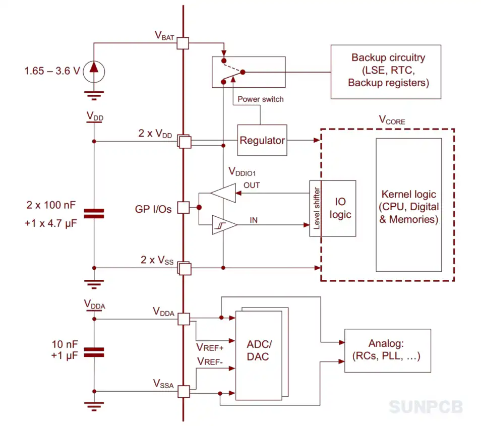
STM32F051R8T6 Power Supply Scheme diagram. (Page 43/122)
While a specific 'Typical Application Circuit' isn't provided, the Power Supply Scheme (Figure 13 in the datasheet) is critical. Engineers must ensure proper decoupling for each power supply pair (VDD/VSS, VDDA/VSSA) using ceramic capacitors placed very close to the pins. VDDA must be greater than or equal to VDD. This schematic is essential for stable operation.
4. STM32F051R8T6 Functional Block Diagram
- ARM Cortex-M0 Core: 32-bit CPU, up to 48 MHz.
- Memory: 64 KB Flash, 8 KB SRAM with parity.
- Timers: 11 timers for PWM, IR, and DAC.
- Communication Interfaces: I2C, USART, SPI, HDMI CEC.
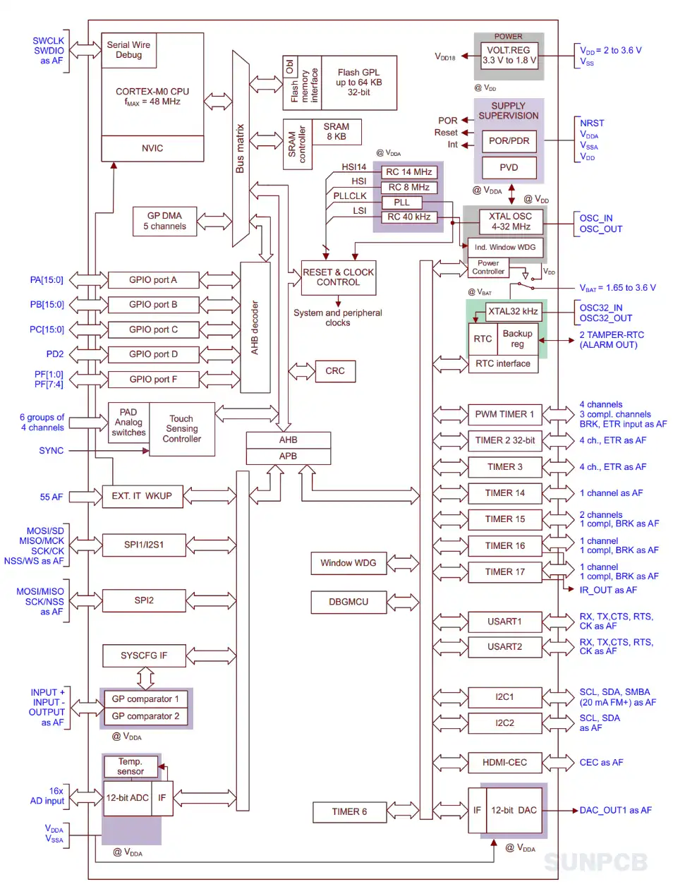
Located on page 12.
![]() STM32F051R8T6 functional block diagram pdf download (P12/P122)
STM32F051R8T6 functional block diagram pdf download (P12/P122)
5. STM32F051R8T6 STMicroelectronics Overview
5.1 Description
The STM32F051R8T6 belongs to the STM32F051xx family, incorporating the high-performance ARM® Cortex®-M0 32-bit RISC core operating at up to 48 MHz frequency. It features high-speed embedded memories (64 Kbytes of Flash, 8 Kbytes of SRAM) and a wide range of enhanced peripherals and I/Os. These devices offer a balance of performance, power consumption, and peripheral features suitable for many applications. They operate from a 2.0 to 3.6 V power supply.
5.2 Overview
The STM32F051R8T6 provides a cost-effective platform meeting MCU implementation needs with reduced pin count and low-power consumption, while delivering outstanding computational performance and advanced interrupt response. The Cortex-M0 core offers exceptional code-efficiency, achieving high performance with memory sizes typically associated with 8- and 16-bit devices. The device integrates memory, timers, ADCs, DACs, communication interfaces, and capacitive sensing capabilities, making it versatile. It supports various boot modes and includes power management features like Sleep, Stop, and Standby modes.
5.3 Features
- Core: ARM® Cortex®-M0 32-bit CPU @ 48 MHz.
- Memories: 64 KB Flash, 8 KB SRAM with HW parity.
- Clock/Reset/Supply Management: 2.0-3.6V VDD, POR/PDR, PVD, Low Power Modes (Sleep, Stop, Standby), VBAT supply. Internal/External Oscillators, PLL.
- I/O: Up to 55 fast I/Os, most 5V-tolerant, mappable to external interrupts.
- DMA: 5-channel DMA controller.
- ADC/DAC/Comparators: One 12-bit 1.0 µs ADC (up to 19 channels), one 12-bit DAC channel, two fast low-power comparators.
- Touch Sensing: Up to 18 capacitive sensing channels.
- Timers: Up to 11 timers including advanced control, general purpose, basic, watchdog, and SysTick timers.
- Communication Interfaces: Up to 2x I2C (one FM+), up to 2x USART (supporting SPI, modem control, ISO7816, LIN, IrDA, auto baud rate), up to 2x SPI (18 Mbit/s, one with I2S). HDMI CEC interface.
- Debug: Serial wire debug (SWD).
- Unique ID: 96-bit unique ID.
These features enable precise control, flexible communication, and low-power operation. Engineers should note the specific capabilities of each peripheral, like the FM+ support on I2C1 and the independent clock domains for some peripherals allowing wakeup from Stop mode.
6. STM32F051R8T6 Parameters
| Specification | Value | Specification | Value |
|---|---|---|---|
| Core Specifications | |||
| Core Architecture | ARM | Data Bus Width | 32 b |
| Frequency | 48 MHz | Max Frequency | 48 MHz |
| Memory | |||
| Flash Memory Size | 64 kB | Memory Size | 64 kB |
| Memory Type | FLASH | RAM Size | 8 kB |
| Power | |||
| Max Operating Temperature | 85 °C | Min Operating Temperature | -40 °C |
| Max Supply Voltage | 3.6 V | Min Supply Voltage | 2 V |
| Max Power Dissipation | 444 mW | Nominal Supply Current | 1.7 µA |
| Interfaces | |||
| Interface | HDMI, I2C, I2S, IrDA, LIN, SPI, UART, USART | Number of I2C Channels | 2 |
| Number of SPI Channels | 2 | Number of USART Channels | 2 |
| Number of I/Os | 55 | Number of Programmable I/O | 55 |
| Analog Features | |||
| Number of A/D Converters | 1 | Number of ADC Channels | 19 |
| Number of Channels | 16 | Number of D/A Converters | 1 |
| Number of PWM Channels | 1 | Number of Timers/Counters | 1 |
| Peripherals | |||
| Peripherals | DMA, I2C, POR, PWM, WDT | Oscillator Type | Internal |
| Watchdog Timer | Yes | ||
| Physical | |||
| Case/Package | LQFP | Contact Plating | Gold, Tin |
| Number of Pins | 64 | Height | 1.45 mm |
| Length | 10.2 mm | Width | 10.2 mm |
| Compliance | |||
| Lead Free | Lead Free | Radiation Hardening | No |
| REACH SVHC | No | RoHS | Compliant |
| Others | |||
| Schedule B | 8542310000 | Lifecycle Status | Production (Last Updated: 4 years ago) |
7. STM32F051R8T6 Electrical Characteristics
| Power Supply & Reset | |||||
|---|---|---|---|---|---|
| Parameter | Min | Typ | Max | Unit | Notes |
| VDD | 2.0 | 3.6 | V | Standard operating voltage. | |
| VDDA (ADC/DAC used) | 2.4 | 3.6 | V | Analog operating voltage. Must be >= VDD. | |
| VPOR/PDR (Falling) | 1.80 | 1.88 | 1.96 | V | Power on/power down reset threshold. |
| VREFINT | 1.2 | 1.23 | 1.25 | V | Internal reference voltage (-40 to +105°C). |
| IDD Run (48MHz, Flash, All Periph. OFF, 3.6V, 25°C) | 11.8 | 12.7 (@85°C) | mA | Typical/Max Run mode current from VDD. | |
| IDD Stop (Regulator LP, All OSC OFF, 3.6V, 25°C) | 4.0 | (See datasheet) | µA | Typical Stop mode current from VDD. | |
| IDD Standby (LSI OFF, IWDG OFF, 3.6V, 25°C) | 1.3 | 2.0 | µA | Typical/Max Standby mode current from VDD. | |
| I/O Characteristics (VDDIOx = 2.7V to 3.6V unless specified) | |||||
| Parameter | Min | Typ | Max | Unit | Notes |
| VIL (FT/FTf I/O) | - | 0.475 VDDIOx–0.2 | V | Input low level voltage. | |
| VIH (FT/FTf I/O) | 0.5 VDDIOx+0.2 | - | V | Input high level voltage. | |
| VOL (|IIO|=8mA) | - | 0.4 | V | Output low level voltage. | |
| VOH (|IIO|=8mA) | VDDIOx–0.4 | - | V | Output high level voltage. | |
| RPU (Weak Pull-up) | 25 | 40 | 55 | kΩ | Pull-up resistor. |
| RPD (Weak Pull-down) | 25 | 40 | 55 | kΩ | Pull-down resistor. |
| ADC (12-bit) | |||||
| Parameter | Min | Typ | Max | Unit | Notes |
| fADC | 0.6 | 14 | MHz | ADC clock frequency. | |
| Sampling Rate | 0.043 | 1 | MS/s | Max sampling rate. | |
| ET (Total Unadjusted Error) | ±1.3 | ±2 | LSB | VDDA=3-3.6V, 25°C. | |
| tCONV (12-bit) | 1 | 18 | µs | fADC = 14 MHz. | |
| DAC (12-bit) | |||||
| Parameter | Min | Typ | Max | Unit | Notes |
| DNL (12-bit) | ±2 | LSB | Differential Non-Linearity. | ||
| INL (12-bit) | ±4 | LSB | Integral Non-Linearity. | ||
| tSETTLING (Buffered) | 3 | 4 | µs | Settling time (full scale, ±1LSB). | |
8. STM32F051R8T6 Layout Example
A specific PCB layout example is not provided in the datasheet, but the recommended footprint for the target package is essential for correct layout design. Below is the placeholder for the recommended footprint for the LQFP64 package.
- Ensure proper power supply decoupling as shown in the Power Supply Scheme (Figure 13). Place decoupling capacitors (e.g., 10nF ceramic) as close as possible to VDD/VSS and VDDA/VSSA pairs.
- Follow the recommended PCB pad dimensions and spacing provided in the footprint details.
- Minimize trace lengths for high-frequency signals like clock lines (HSE/LSE). Place crystals/resonators and load capacitors very close to the MCU pins.
- Consider grounding strategies, especially for mixed-signal designs involving the ADC or DAC, connecting VSSA appropriately.
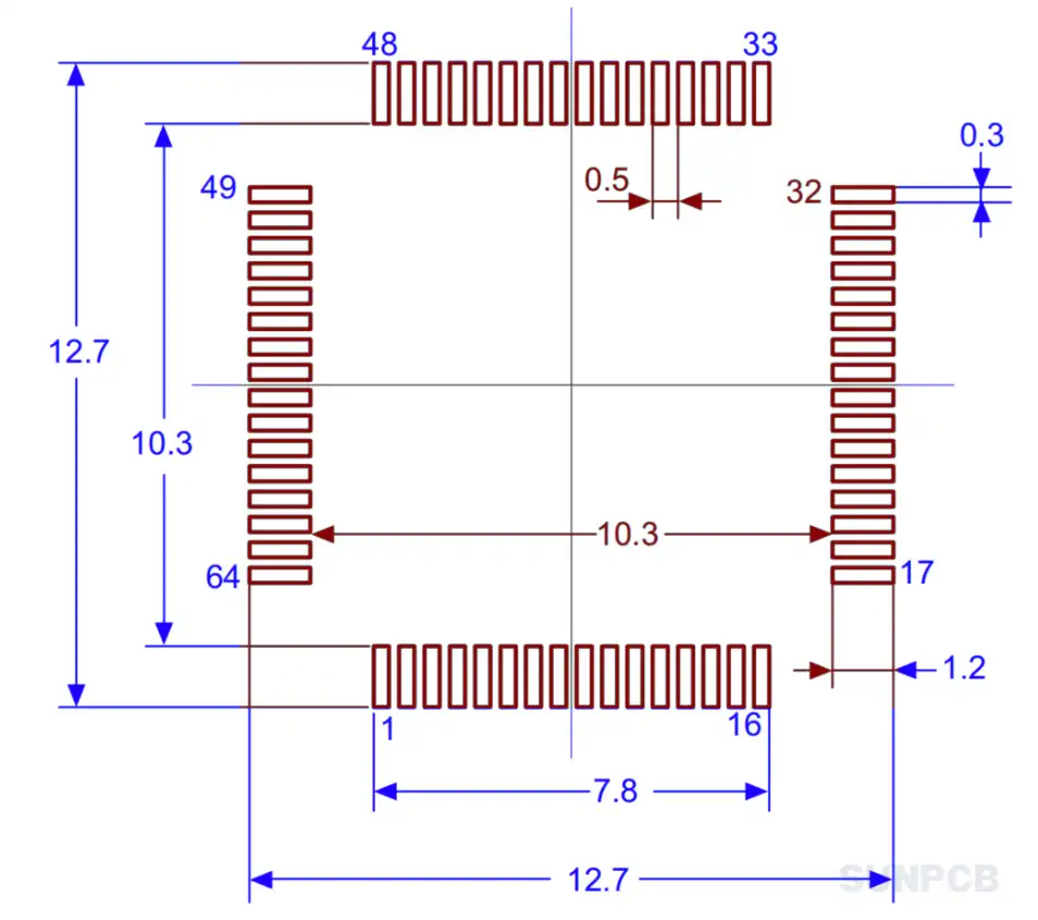
9. STM32F051R8T6 Package Example Dimension - LQFP-64
The STM32F051R8T6 is available in an LQFP-64 package, which is a low-profile quad flat package with 64 pins and dimensions of 10x10 mm body size and 0.5 mm lead pitch. Engineers must refer to the detailed mechanical data (Table 67) and the package outline drawing (Figure 37) for precise dimensions required for PCB footprint design and assembly processes. Key dimensions include package height (Max 1.6mm), lead width (0.17-0.27mm), and body size (10x10mm typ). Understanding these dimensions ensures compatibility with manufacturing constraints.
Engineer Notes: Check pin spacing and thermal pad needs during layout.
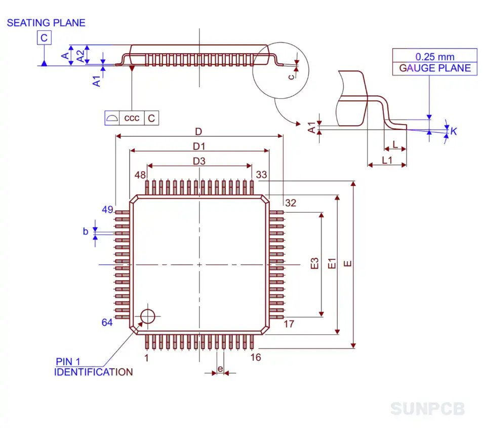
STM32F051R8T6 LQFP-64 Package Located on page 94.
10. STM32F051R8T6 Part Numbering System
The ordering information scheme helps decode the part number.
| Field | Example | Description |
|---|---|---|
| Device Family | STM32 | ARM-based 32-bit microcontroller |
| Product Type | F | General-purpose |
| Sub-family | 051 | STM32F051xx |
| Pin Count | R | R = 64 pins (K=32, T=36, C=48) |
| Memory Size | 8 | 8 = 64 Kbyte Flash (4=16KB, 6=32KB) |
| Package | T | T = LQFP (H=UFBGA, U=UFQFPN, Y=WLCSP) |
| Temperature Range | 6 | 6 = –40°C to +85°C (7 = –40°C to +105°C) |
| Options | (TR or blank) | Packing type (TR=Tape & Reel, blank=Tray) or programmed part code |
11. STM32F051R8T6 FAQs and Tips
FAQs
Q: What is the core of the STM32F051R8T6?
A: It uses the ARM® Cortex®-M0 32-bit RISC core.
Q: What is the maximum operating frequency?
A: The maximum CPU frequency is 48 MHz.
Q: What are the memory specifications?
A: It has 64 KB of Flash memory and 8 KB of SRAM.
Q: What is the operating voltage range?
A: The main supply voltage (VDD) range is 2.0V to 3.6V. The analog supply (VDDA) must be between VDD and 3.6V (minimum 2.4V if ADC/DAC are used).
Q: What key peripherals are included?
A: Key peripherals include multiple Timers (Advanced, GP, Basic), Communication interfaces (SPI, I2C, USART, CEC), a 12-bit ADC, a 12-bit DAC, Comparators, DMA, RTC, and Watchdogs.
Q: What debug interface is supported?
A: It supports Serial Wire Debug (SWD).
Q: Does it support low-power operation?
A: Yes, it supports Sleep, Stop, and Standby low-power modes.
Q: What package does the 'R8T6' variant come in?
A: STM32F051R8T6 specifically refers to the LQFP64 package.
Tips
- Consult Documentation: The Reference Manual (RM0091) is essential for detailed register and peripheral information. Datasheets provide electrical specs, and Application Notes offer guidance on specific functions (e.g., oscillator design AN2867).
- Utilize ST Tools: Use STM32CubeMX for peripheral configuration and code generation (HAL or LL drivers). STM32CubeIDE integrates development and debugging.
- Power Supply Design: Pay close attention to power supply decoupling. Place decoupling capacitors close to the VDD/VSS and VDDA/VSSA pins. Ensure VDDA ≥ VDD.
- Clock Management: Carefully select and configure clock sources (HSI, HSE, LSI, LSE, PLL) based on application requirements for performance and power consumption. Place external crystals/resonators and capacitors close to pins.
- Low-Power Modes: Leverage Sleep, Stop, and Standby modes to minimize power consumption. Understand wakeup sources and latency.
- RTOS Considerations: If using a Real-Time Operating System (RTOS), understand task scheduling and interrupt handling specific to the Cortex-M0 and chosen RTOS. The SysTick timer is dedicated for RTOS use.
- Start Simple: Begin with development boards like Nucleo or Discovery kits which include onboard debuggers (ST-LINK) before designing custom hardware.