SUNPCB provides precision-engineered PCB solutions that power mission-critical innovation across the Medical, Automotive, Industrial, Cloud Computing, Communications, Energy, and Networking sectors, where advanced technology meets uncompromising reliability.
| Feature | Capability |
|---|---|
| Via Types | Blind via, buried via, through-hole via |
| Number of layers | Up to 60 layers (evaluation required above 30 layers) |
| HDI builds | 1+N+1, 2+N+2 , ... , 6+N+6 (≥6 orders require evaluation) |
| Copper weights (finished) | 18 um ~ 70 um |
| Min trace/spacing | 0.065 mm / 0.065 mm |
| PCB thickness | 0.1 ~ 8.0mm (evaluation required for less than 0.2 mm or greater than 6.5 mm) |
| Max. PCB dimension (finished) | 2 ~ 20 layers, 21*33 inches; length ≤ 1000 mm; evaluate if short side > 21 inches |
| Feature | Capability |
|---|---|
| Min. mechanical drilling | 0.15 mm |
| Min. laser drilling | Standard 4 mil, 3 mil require evaluation (corresponding to single 106PP). |
| Max. laser drilling | 8 mil (corresponding dielectric thickness cannot exceed 0.15mm) |
| Min. controlled depth drilling | PTH: 0.15 mm; NPTH: 0.25 mm |
| Aspect ratio | Max 14:1; evaluate if greater. |
| Min. solder mask bridge | 4 mil (green, ≤1 OZ)5 mil (other colors, ≤1 OZ) |
| Diameter range of resin-filled vias | 0.254 ~ 6.5 mm |
Leveraging advanced laser drilling and precision multilayer stacking, our HDI PCBs deliver ultra-high density, reliability, and miniaturization for cutting-edge applications across Medical, Automotive, Industrial, Cloud Computing, Communications, Energy, and Networking sectors. With decades of expertise in microvia technology and blind/buried via designs, we ensure superior signal integrity and thermal performance for high-speed, high-frequency systems. Rigorous quality control (IPC Class 3 standards) and flexible manufacturing capabilities empower us to meet complex project demands, from prototypes to mass production. Trust our ISO-certified HDI solutions to accelerate your product's time-to-market with uncompromising precision.


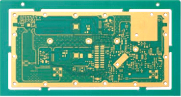
* All product case studies on this site are client-authorized.
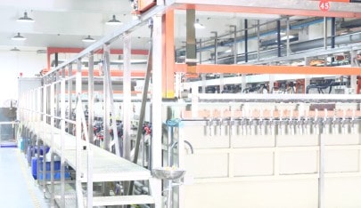
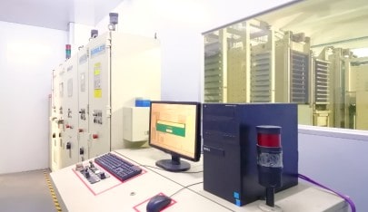
SUNPCB's factory leverages high-precision equipment meeting aerospace standards, with machinery achieving tolerances as low as ±0.05 mm and line widths down to 75 microns. Integrated with Industry 4.0, our production lines feature real-time analytics and smart controls for efficient, responsive manufacturing.
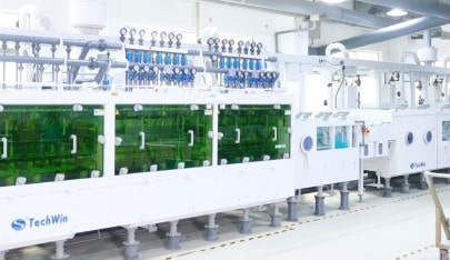
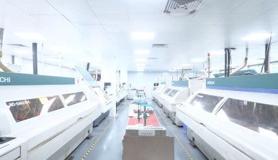
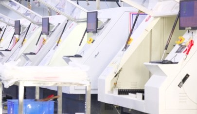
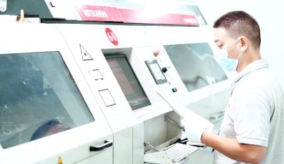
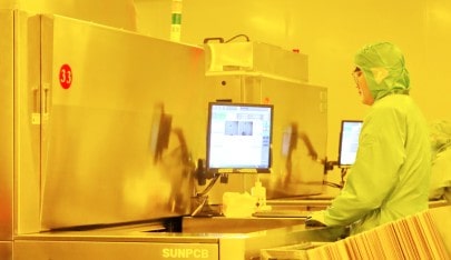
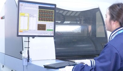
Our PCB factory delivers exceptional quality through advanced engineering and inspection processes, supported by highly experienced teams. From optimized design-to-production workflows and precise optical inspections to efficient electrical testing and rigorous quality control, we ensure compliance with industry standards for top-tier reliability and performance.


Linking Innovation to Reality
SUNPCB, based in Canada, is a global PCB & EMS solutions leader with 10+ years of expertise, offering end-to-end services from prototyping to mass production.

